
48Vdc &220Vdc Modular parallel inverter Without Battery Pure Sine Wave Inverter 3kw Modular Inverter
19 Inch 110Vdc & 220Vdc Parallel Inverter Manual user Parallel inverter power supply
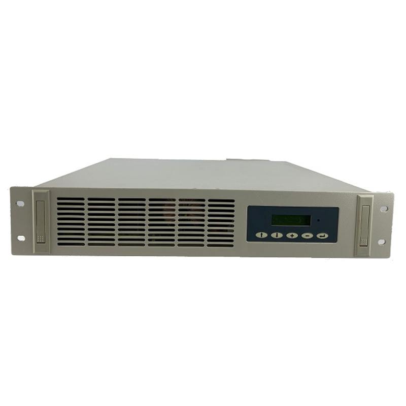
DC 48V 10000 Watt inverter 10KVA pure wave sine power inverter telecom 4U rack mount inverter

Embedded Power System 3u dc 48v 150A switching power supply
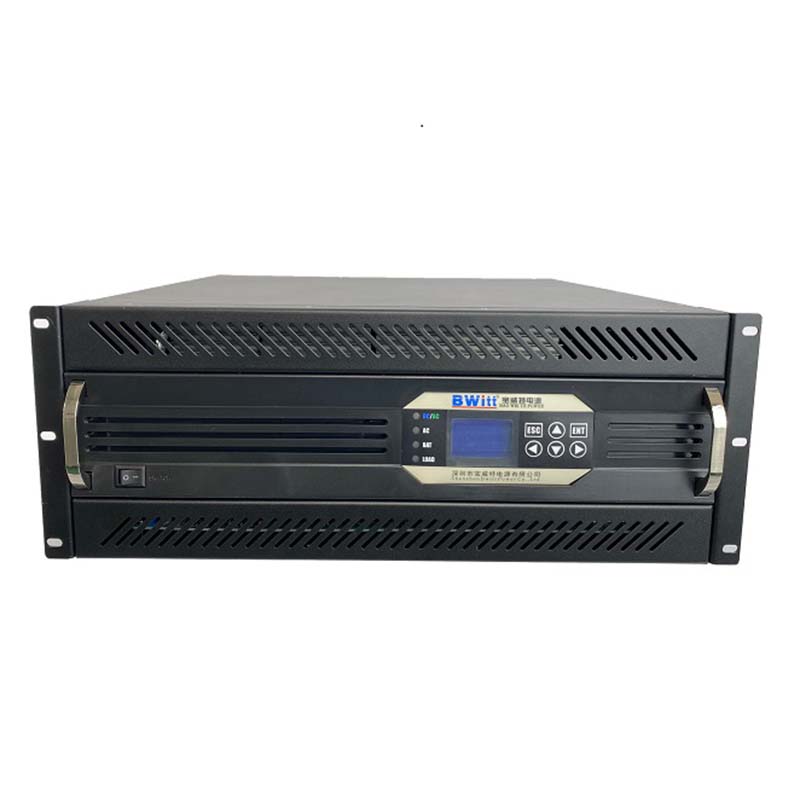
Single-phase Bwitt 48v to AC220v 1000w pure sine wave inverter 1000w inverter with snmp

With the continuous advancement of science and technology, inverter technology has developed more extensively. Research on inverter power supplies has also developed further. At present, in addition to power frequency inverters, high-frequency inverters have also begun to occupy the development market of inverter power supplies and are expected to replace power frequency inverters. Although high-frequency inverters make up for the shortcomings of power frequency inverters such as large size, low frequency, and low efficiency, they still cannot completely replace the role of power frequency inverters. Compared with high-frequency inverters, power frequency inverters have their own unique advantages. An independent inverter power supply design scheme based on power frequency transformer is proposed here.
1. Inverter power supply structure design
Figure 1 is a block diagram of an inverter power supply based on pulse width modulation (PWM) technology. The entire circuit selects low-voltage DC input and inverts it to AC voltage through the full-bridge inverter circuit. It is boosted to the rated peak value by the power frequency boost circuit, and then the AC voltage that meets the requirements is output through the filter circuit. Generally, it is required to output 220V/50Hz AC.
2. Inverter power supply hardware circuit design
2.1 PWM technology
The theoretical basis of PWM control technology is the impulse theorem. The sine wave is used as the modulation wave to apply a bipolar pulse width modulation wave (SPWM) with the same carrier output amplitude and the pulse width changes according to the sine wave. This square wave signal is added to the inverse The variable bridge inverter power tube is controlled to turn on and off, and finally a close to ideal AC output waveform is obtained. This technology makes the hardware circuit simple and improves the output waveform efficiency. Figure 2 is the wiring diagram and SPWM waveform using the U3988 device to control the inverter bridge. 0UTA and 0UTB are the output pins of the sine wave SPWM pulse sequence. The signals output by these two pins generally need to pass through the dead control circuit before being sent to the inverter. Change bridge.
2.2 The role of power frequency transformer in inverter circuit
The input of power frequency inverter power supply is generally low-voltage DC, which uses a full-bridge inverter circuit to control the output AC voltage by affecting the switching frequency of the field effect tube. The peak-to-peak value of the output 220V sine wave AC voltage is 620V, while the input rectified voltage of the general inverter power supply is 310V. In order for the inverter to output the 220V sine wave AC voltage without distortion, the DC voltage in front of the inverter must be 680 ~870V. Because the general inverter input voltage is much smaller than this value, an output transformer must be added to increase the inverter output voltage above the rated peak value before it can be used, as shown in Figure 3.
This circuit adopts a full-bridge conversion circuit structure. The output of this converter is not one live wire and one neutral wire, but two live wires. However, a neutral wire is generally required when connecting to a load. If there is no output isolation transformer and the live wire is rigidly connected to the neutral wire, the inverter power supply will not work properly. Figure 4 shows the current flow direction during the positive half wave of the non-output transformer.
It can be seen from Figure 4 that due to the access of the neutral line, the load current does not pass through the rectifier tube and the inverter power tube after passing through the load, but flows directly back to the neutral line input terminal of the mains. In this case, Figure The rectifier and inverter power tube in the middle dotted box are not functioning. According to the normal working procedure, the load current should flow through the rectifier tube and inverter power tube of the two bridge circuits. Figure 5 shows the current flow direction when there is a positive half wave of the output transformer. When the output end is connected to an isolation transformer, the secondary (load input end) of the transformer can be connected to the neutral line of the mains power, thus forming a reliable power supply system. It can be seen that the isolation output transformer is an important component of the inverter bridge circuit, making the inverter circuit reliable and stable.
2.3 Protection circuit
U3988 has built-in reference voltage for undervoltage protection and overheating protection. It only needs to divide the voltage through resistors. When the voltage is lower than the reference voltage, U3988 will be locked to stop outputting pulses. In addition, in terms of current protection, depending on the load current, there are three-stage protection functions: fast protection, short delay and long delay.
3. Shortcomings of inverter power circuit
The isolation transformer is connected for the purpose of transforming voltage and isolating the neutral line, and does not have the function of isolating interference and buffering load mutation. There is an insulating layer between the primary and secondary of the transformer. They form a capacitor C with a certain capacity. The capacitive reactance of the capacitor is inversely proportional to the frequency, that is:
In the formula, Xc is the capacitive reactance of the equivalent distributed capacitance between the primary and secondary transformers, in Ω. f is the frequency of the interference signal, in Hz. C is the equivalent distributed capacitance between the primary and secondary of the transformer, in F.
It can be seen from equation (1) that the higher the frequency, the smaller the capacitive reactance, that is, the higher the frequency of the interference signal, the easier it is for the capacitive path to pass through. Since the frequency of general interference signals is very high, they can be driven directly through the transformer to interfere with the load. If lower frequency interference comes, it will change the interference load proportionally according to the transformation ratio of the transformer. Since the transformer does not have an anti-interference function, input and output filters are generally added to the input and output ends of the inverter bridge.
Due to the connection of the isolation transformer, low-frequency devices such as inductors and capacitors will be connected, which not only increases the size of the circuit itself but also increases the power consumption of the circuit and reduces the output efficiency of the circuit. With the gradual development of high-frequency and low-priced devices such as electronic transformers, the production cost of power frequency transformers has increased relatively, and the production cost of circuit boards designed for this system has also increased accordingly.
4 Conclusion
Through the above analysis, the circuit structure and characteristics of the power frequency inverter power supply are comprehensively introduced. This designed circuit combines the advanced functions of digital devices and the isolation function of the power frequency transformer to achieve the purpose of simple and reliable circuit design.
Bwitt is the world's leading provider of rack-mounted telecom inverters and modular DC power rectifier system factories.
INQURY9 / F, Building 20 Ericsson Industrial Park, No. 19, Huifeng East 1st Road Zhongkai High-tech Zone, Huizhou City Guangdong Province China